Q1
- Design a logical circuit with:
- Inputs: 8 bits
- 3 control bits ().
- Outputs: 8 bits
- The circuit performs a left circular shift (Left Rotate) on the input bits by a value , determined by the control bits .
- In a left circular shift, bits shifted out from the left end re-enter from the right end.
- You may use a schematic representation for your solution. There’s no need to draw all connections, but the schematic and explanation should clarify how each input bit is routed to produce the output.
- Example: For , one left circular shift moves the most significant bit (MSB) to the least significant bit (LSB) position.
- Refer to basic components from Chapter 5 for your design.
Q2
- Refer to Diagram B.8.4 in Appendix B (Page 132 of the study guide).
- Explain the term falling-edge triggered
- What happens to the circuit if the clock remains constantly in the high (1) state? (asserted)
- What happens if the NOT gate at the input to the slave latch is removed?
- Refer to Diagram B.8.6 in Appendix B (Page 133 in SG), and B.11 section.
- Define “Setup Time” and “Hold Time” concepts.
Q3
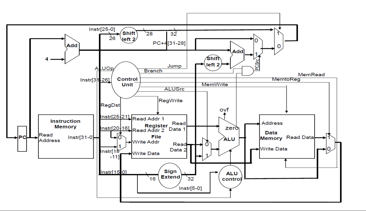
Control Signals for Instruction narrative (in MIPS single-cycle processor):
| RegDst | ALUSrc | MemtoReg | RegWrite | MemRead | MemWrite | Branch | ALUOp1 | ALUOp0 |
|---|---|---|---|---|---|---|---|---|
| 1 | 0 | 1 | 1 | 1 | 0 | 0 | 0 | 1 |
- What does the instruction
narrativedo? What values are written and where? (Use Diagram 4.24 and Table 4.18).- Calculate the written values assuming:
- rt (bits 16–20) = 12
- rs (bits 21–25) = 14
- rd (bits 11–15) = 3
- Register values are initialized as
R[i] = i^2(e.g.,R8 = 64, R10 = 100).
- Calculate the written values assuming:
- Memory addresses from
0to1000contain the value0xA5- Is it possible to implement this instruction in MIPS? If yes, which format would it use? If not, explain why.
Q4
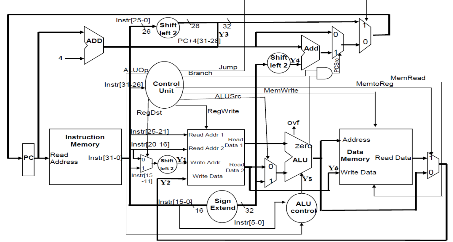
You are given the following MIPS assembly code snippet:
| Address | Code | Basic | Source |
|---|---|---|---|
0x74007484 | 0x2063fd00 | addi $3, $3, -768 | addi $3, $3, -0x300 |
0x74007488 | 0xac6c0800 | sw $12, 2048($3) | sw $12, 0x800($3) |
0x7400748c | 0x8da2fe00 | lw $2, -512($13) | lw $2, -0x200($13) |
- Each register starts with the value
0x10010000plus its register number multiplied by0x100. For example:$1=0x10010100$2=0x10010200$3=0x10010300$4=0x10010400- (and so on, except
$0, which is always0).
- All memory addresses are accessible for
swandlwinstructions, provided the address is a multiple of 4. - Processor Modifications:
- A 2-bit left shift unit is added to the processor. This unit is connected to the output of the
RegDstmultiplexer. - The left shift moves the bits of its input two places to the left and fills the two rightmost bits with zeros (bits shifted out on the left are discarded).
- A 2-bit left shift unit is added to the processor. This unit is connected to the output of the
- Task:
- For the given third instruction (
lw $2, -512($13)), determine the values on the six highlighted lines (markedY1toY6) in hexadecimal. - Use the processor diagrams and data from Tables 4.12 and 4.18 (pages 169–170 of the SG) to assist in the calculations.
- If a value is unknown, mark it as
X.
- For the given third instruction (
- Notes:
- Line
Y3corresponds to(PC + 4) (bits 28–31). - The effect of the 2-bit left shift unit must also be considered for prior instructions.
- Line

Q5
Add a jm (memory jump) instruction to the single-cycle processor’s datapath.
- The instruction jumps to the memory word at the address specified by
- Instruction Format:
jm IMM($rs) - Tasks:
- Draw the instruction fields (e.g., opcode, registers, immediate) and show required changes to Diagram 4.24 and Table 4.18. Add components if necessary.
- Discuss whether it’s possible to extend the immediate/offset field for this instruction and what would be required to do so.
- Refer to the existing instructions (e.g.,
addi,jump) in Table 4.18 as examples. - You need to add the
jm(memory jump) instruction to the single-cycle datapath. The instruction causes a jump based on the value of a word fetched from the data memory, where the address is specified in the instruction. The instruction is composed of a register ($rs) and an offset (IMM) of 16 bits, after sign extension. The instruction format is:jm IMM($rs) - The result is a jump to
MEM[$rs + sign_extend(IMM)]
| Instruction | Opcode | RegDst | ALUSrc | MemtoReg | RegWrite | MemRead | MemWrite | Branch | ALUOp1 | ALUOp0 | Jump |
|---|---|---|---|---|---|---|---|---|---|---|---|
| R-Type | 0 | 1 | 0 | 0 | 1 | 0 | 0 | 0 | 1 | 0 | 0 |
| lw | 35 | 0 | 1 | 1 | 1 | 1 | 0 | 0 | 0 | 0 | 0 |
| sw | 43 | x | 1 | x | 0 | 0 | 1 | 0 | 0 | 0 | 0 |
| beq | 4 | x | 0 | x | 0 | 0 | 0 | 1 | 0 | 1 | 0 |
| addi | 8 | 0 | 1 | 0 | 1 | 0 | 0 | 0 | 0 | 0 | 0 |
| j | 2 | x | x | x | 0 | 0 | 0 | x | x | x | 1 |
| jm | 63 (0x3F) |
