Boolean Algebra
-
A logic function (or Boolean function) is a function that takes bits of input and produces a single bit of output.
- Representations:
- Truth table that contains rows (one for each possible combination of inputs) and columns (one for each input and one for the output)
- Logic equation that represents the function in using other logic functions, especially, as:
- Sum-of-products (SOP)
- Product-of-sums (POS)
- An expression that uses only AND, OR, and NOT
- Simplification:
- Karnaugh map (K-map)
- Quine–McCluskey algorithm
- Algebraic manipulation
- Representations:
-
A logic gate (or simply gate) is a device that implements a logic function.
-
A logical expression
-
A logic equation
-
Two logic expressions are equivalent if
Transformation from truth table to either SOP or POS form:
Truth table SOP:
- Find the miniterms for each row for which the output is 1
- Sum (ORing) all the miniterms
Truth table POS:
Find the mintems for each row for which the output is 0
Find the complement of the sum of the miniterms
Use De Morgan’s laws to change miniterms to maxterms
Example:
Given the truth table:
0 0 1 0 1 0 1 0 1 1 1 1 (SOP) (POS)
Logic Gates
\documentclass{standalone}
\usepackage{circuitikz}[american]
\usetikzlibrary{matrix}
\tikzset{every node/.style={line width=0.2mm}} % Change the thickness here

\begin{document}
\sffamily
\begin{circuitikz}
    % Define the matrix layout with 3 columns and 2 rows, and name each node
    \matrix[matrix of nodes, column sep=3cm, row sep=1.2cm, nodes={anchor=center}] (m) {
        \node[buffer port] (buffer1) {}; & \node[not port] (not1) {}; \\
        \node[and port] (and1) {}; &  \node[nand port] (nand1) {}; \\
        \node[or port] (or1) {}; & \node[nor port] (nor1) {}; \\
		\node[xor port] (xor1) {}; & \node[xnor port] (xnor1) {}; \\
    };

	\node[left of=buffer1, xshift=-1cm] {BUFFER};
    \node[left of=and1, xshift=-1cm] {AND};
    \node[left of=or1, xshift=-1cm] {OR};
    \node[left of=not1, xshift=-1cm] {NOT};
    \node[left of=nand1, xshift=-1cm] {NAND};
    \node[left of=nor1, xshift=-1cm] {NOR};
    \node[left of=xor1, xshift=-1cm] {XOR};
    \node[left of=xnor1, xshift=-1cm] {XNOR};
\end{circuitikz}
\end{document}| Logical operation | Operator | Notation | eq. form |
|---|---|---|---|
| NOT | |||
| logical sum | OR | ||
| logical product | AND | ||
| NAND | |||
| NOR | |||
| XOR | |||
| XNOR |
Laws
- Identity law:
- Zero and one law: (Annihilator)
- Inverse law: (Complemention)
- Commutative law:
- Associative law:
- Distributive law:
- Double negation:
- De Morgan’s laws:
Logic Circuits
-
logic circuits
- a combinational logic (מעגל צירופי) is a device consisting of logic gates whose outputs at any time are determined by the current inputs
- a sequential logic (מעגל סדרתי) is a device consisting of logic gates whose outputs at any time are determined by the current inputs and the previous state of the device
-
packaged building-block logic families can be divided into categories:
- resistor-transistor logic (RTL) circuits are logic circuits built from resistors and transistors
- diode-transistor logic (DTL)
- transistor-transistor logic (TTL)
-
An integrated circuit (IC) is a device that contains many logic gates on a single chip of silicon
- ICs have external electrical contact points called pins
- A package is a plastic or ceramic case that holds the IC and connects the pins to the outside world
- A dual in-line package (DIP) is a package with two parallel rows of pins
-
A discrete component is an electronic device containing only a single element, such as a transistor or a resistor
Combinational Logic
Decoder
- A -bit decoder is a logic block that takes an -bit input and activates one of outputs
- are the output lines
- input lines
- If the value of the input is , then the -th output will be true, and all other outputs will be false
Example: 3-bit decoder
Only the output corresponding to the binary value of the input is true, as shown in the truth table. The label 3 on the input to the decoder says that the input signal is 3 bits wide.
Encoder
- There is also a logic element called an encoder that performs the inverse function of a decoder, taking input and producing an -bit output
Example: 4-to-2 encoder
0 0 0 1 0 0 0 0 1 0 0 1 0 1 0 0 1 0 1 0 0 0 1 1
- Out of 16 possible input values (4 bits), only 4 are valid, so the others are invalid
- A possible implementation of a 4-to-2 encoder (using two OR gates) is:
- Note that the input is not wired
Priority Encoder
- A priority encoder is an encoder
Enable
- An enable (E) is sometimes added to some combinational logic components, when its value is 1, the component is working as usual, but when it is 0, the component is disabled and all its outputs are 0
Exercise
Implement a 3-to-8 decoder using two 2-to-4 decoders that have an enable input. (how can we implement an enable over the 2-to-4 decoder?)
Multiplexor
- A -to- multiplexor (or multiplexer, mux, data selector) is a logic block consisting of:
- data inputs lines labeled
- select lines (or control lines) labeled
- A single output line
- The multiplexor selects the input line if the binary value formed by concatenating the select lines is , and outputs the value of the selected input line (without modification)
- An implementation of a multiplexor with data inputs (and select lines) basically consists of three parts:
- A -bit decoder, where each one (of ) output lines corresponds to one of the data inputs
- An array of AND gates, each combining one of the data inputs with the corresponding decoder output
- An OR gate that combines the outputs of the AND gates to produce the final output
Example: 2-to-1 multiplexor
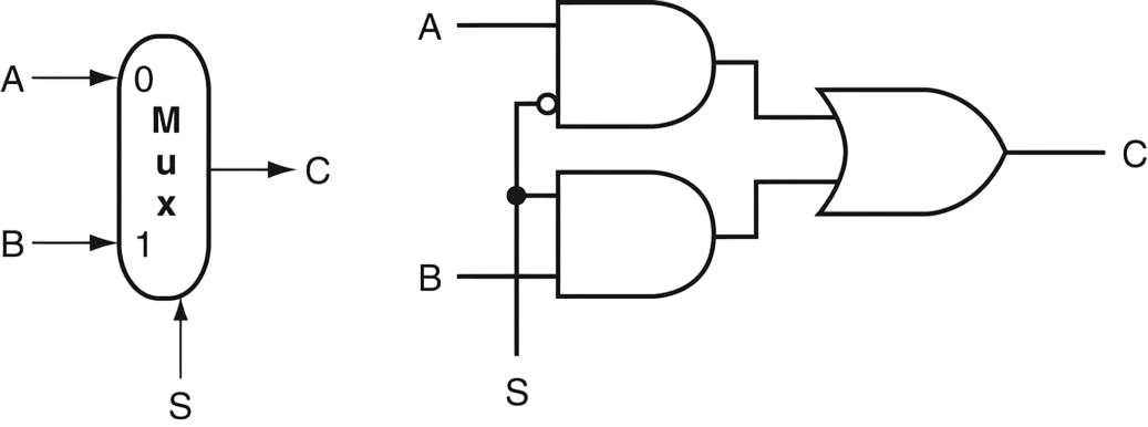
- (left) A 2-to-1 multiplexor with two data inputs ( and , labeled and ), a select line , and an output .
- (right) Its implementation using logic gates, which can be represented by
The truth table of the 2-to-1 multiplexor is:
0 1
Exercise: 4-to-1 multiplexor
Draw an implementation using logic gates of 4-to-1 multiplexor with four data inputs (), two select lines (), and an output .
PLA
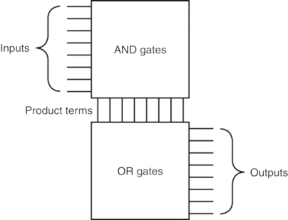
- A programmable logic array (PLA) is a structured-logic elemement that composed of:
- A set of inputs and corresponding input complements
- Two stages of logic:
- (first) an array of AND gates that generate a set of product terms (minterms) of the inputs and their complements
- (second) an array of OR gates that generate sum terms of the product terms, which are the outputs of the PLA
- PLAs implement logic functions as a sum of products (SOP)
PLA Example
In Out A B C D E F 0 0 0 0 0 0 0 0 1 1 0 0 0 1 0 1 0 0 0 1 1 1 1 0 1 0 0 1 0 0 1 0 1 1 1 0 1 1 0 1 1 0 1 1 1 1 0 1
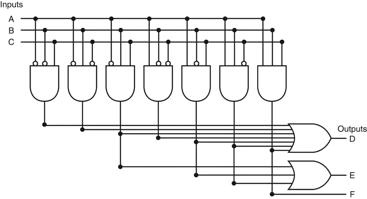
- Since there are 7 unique product terms (with at least one true output), there will be 7 columns in the AND plane
- There are 3 rows in the AND plane (one for each input)
- There are 3 rows in the OR plane (one for each output)
Rather than drawing all the gates, designers often show just the position of AND gates and OR gates.
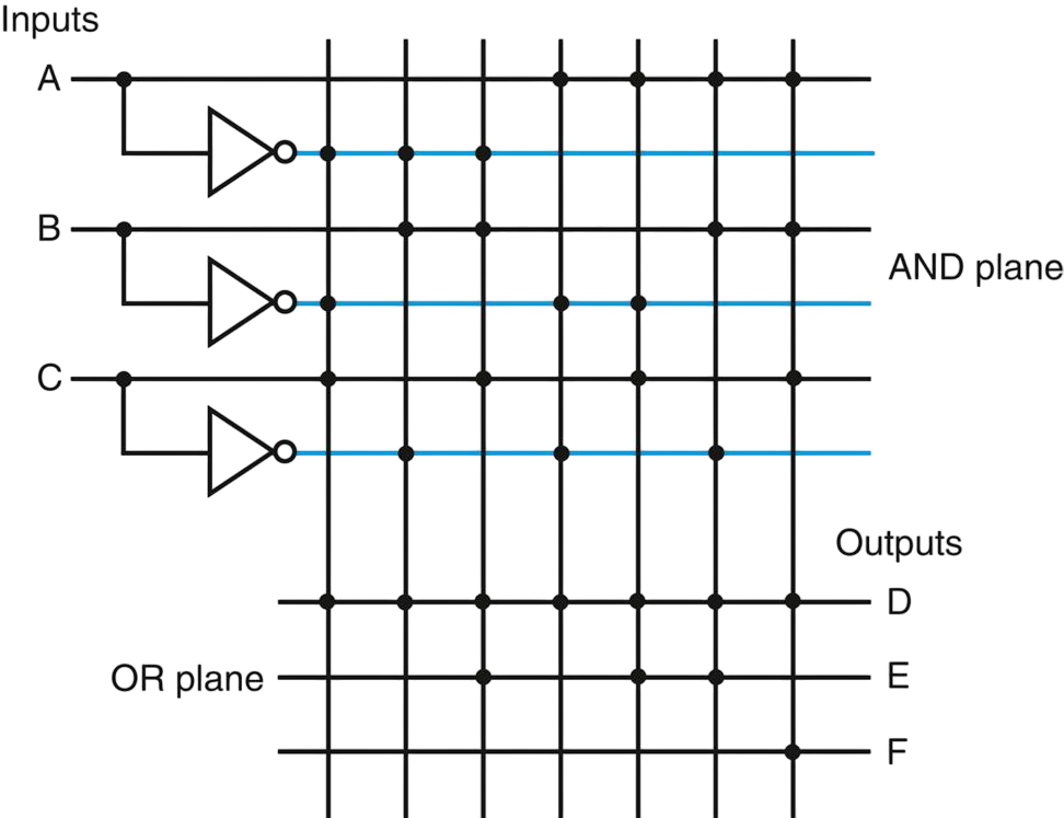
- Rather than use inverters on the gates, usually all the inputs are run the width of the AND plane in both true and complement forms.
- Dots are used on the intersection of a product term signal line and an input line or an output line when a corresponding AND gate or OR gate is required.
- A dot in the AND plane indicates that the input, or its inverse, occurs in the product term.
- A dot in the OR plane indicates that the corresponding product term appears in the corresponding output.
INFO
The contents of a PLA are fixed when the PLA is created, although there are also forms of PLA-like structures, called PALs, that can be programmed electronically when a designer is ready to use them.
ROM
- A read-only memory (ROM) is a memory device with fixed contents that can only be read, typically set at manufacturing.
- The shape (or dimensions) of a ROM is defined by:
- The height which is the number of addressable entries
- (where is the number of input lines)
- The width which is the number of bits in each entry, equal to the number of output bits
- The totel number of bits is
- The height which is the number of addressable entries
- In our context, ROMs are used as structured logic to implement logic functions, where inputs represent addresses, and outputs are the data stored at those addresses.
- The shape (or dimensions) of a ROM is defined by:
Comparison between PLA and ROM for implementing logic functions
- ROMs are fully decoded, meaning:
- they store outputs for all possible input combinations, which results in exponential growth of entries with more inputs.
- they are more flexible since they can implement any logic function with matching input and output sizes, without changing the ROM size
- PLAs are partially decoded, meaning:
they store outputs for only the active product terms, thus, they are generally more efficient for implementing combinational logic functions
EXAMPLE
Following the previous truth table example, the PLA contains only the 7 active product terms, whereas the ROM contains all 8 possible entries.
Programmable ROM
- A programmable ROM (PROM) is a type of ROM that can be programmed electronically after manufacturing when the designer determines its contents.
- A erasable PROM (EPROM) is a programmable ROM that can be erased using ultraviolet light, allowing reprogramming during the design and debugging process.
Don’t Cares
- A don’t care refers to a condition where the specific value of a variable (input or output) does not impact the operation or behavior of a system. This allows flexibility in logic optimization to minimize complexity.
- An output don’t care occurs when the output value of a logic function is irrelevant for a particular input combination. This provides freedom to assign any value to the output for such cases to simplify the overall logic.
- An input don’t care arises when certain inputs have no effect on the output for a specific combination of other inputs. In such cases, the input values can be treated as irrelevant (don’t care), which enables further optimization of the logic.
Example
Consider a logic function, defined as follows:
- If A or B is 1, the output D is 1 (whatever the value of C)
- If A or C is 1, the output E is 1 (whatever the value of B)
- Output F is 1 if exactly one of the inputs is 1, although we do not care about F whenever D and E are both 1.
Here is the full truth table (without don’t cares):
In Out 0 0 0 0 0 0 0 0 1 1 0 1 0 1 0 0 1 1 0 1 1 1 1 0 1 0 0 1 1 1 1 0 1 1 1 0 1 1 0 1 1 0 1 1 1 1 1 0 The truth table written with output don’t cares look like this:
In Out 0 0 0 0 0 0 0 0 1 1 0 1 0 1 0 0 1 1 1 1 1 1 1 1 1 1 1 1 1 1 1 1 1 If we also use the input don’t cares, this truth table can be further simplified to:
In Out 0 0 0 0 0 0 0 0 1 1 0 1 0 1 0 0 1 1 1 1 1 1 1 1 1
INFO
Logic minimization is critical to achieving efficient implementations. One tool useful for hand minimization of random logic is the Karnaugh map. Nevertheless, hand optimization of significant logic functions using K-maps can be challenging, both because of the size of the maps and their complexity, for this reason, design tools are used to automate the process.
Bus
- A bus is a collection of data lines that is treated together as a single logical signal.
- (The term bus is also used to indicate a shared collection of lines with multiple sources and uses.)
- Thick lines in diagrams indicate buses. Width of buses (e.g., 32 bits) may be explicitly labeled.
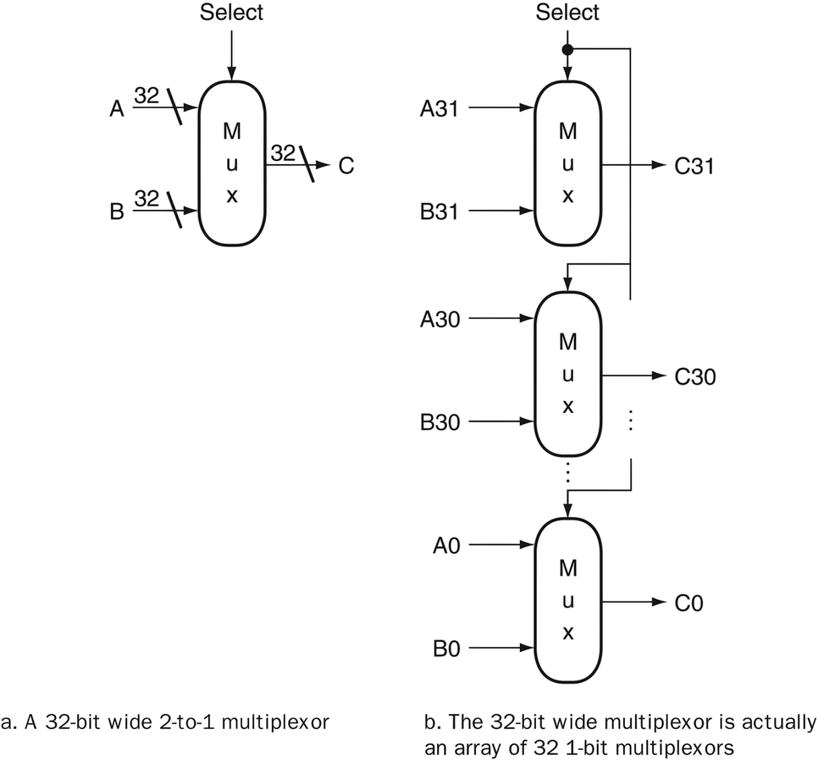
- An array of logic elements
Example: A 32-bit multiplexor
A multiplexor is arrayed 32 times to perform a selection (using one select line) between two 32-bit inputs.
Arithmetic logic circuits
Binary adders
Half Adder
- A half adder addes two single binary digits and , and outputs a sum bit and a carry out bit
- (sum)
- (carry out) (represents an overflow into the next digit of a multi-digit addition)
| In | Out | ||
|---|---|---|---|
| (XOR) | (AND) | ||
| 0 | 0 | 0 | 0 |
| 0 | 1 | 1 | 0 |
| 1 | 0 | 1 | 0 |
| 1 | 1 | 0 | 1 |
Full Adder
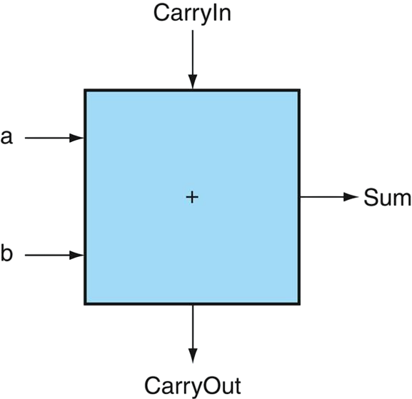
- A full adder adds two bits and and accounts for values carried in as well as out, and outputs a sum bit and a carry out bit
| In | Out | |||
|---|---|---|---|---|
| 0 | 0 | 0 | 0 | 0 |
| 0 | 0 | 1 | 1 | 0 |
| 0 | 1 | 0 | 1 | 0 |
| 0 | 1 | 1 | 0 | 1 |
| 1 | 0 | 0 | 1 | 0 |
| 1 | 0 | 1 | 0 | 1 |
| 1 | 1 | 0 | 0 | 1 |
| 1 | 1 | 1 | 1 | 1 |
Ripple-carry adder
Carry-lookahead adder
ALU
ALU: Summary
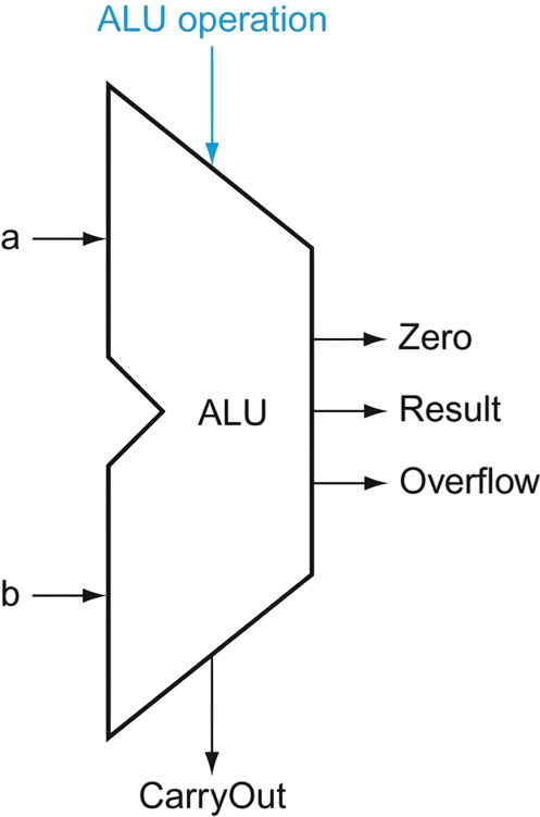
Function Ainv. Binv. Op. Control Dec Output AND 000000000 Result = A AND B OR 000100011 Result = A OR B add 001000102 Result=A+B, subtract 011001106 Result=A-B, slt 011101117 Result0 = 1 if A < B, else 0 NOR 1100110012 Result = A NOR B Here is a summary of the final 32-bit ALU: Inputs
- and are the two 32-bit operands.
- is a 4-bit control line that selects the operation to be performed.
- 1 bit for Ainvert
- 1 bit for Binvert (Bnegate)
- 2 bits for the operation.
00AND01OR10ADD11SLTOutputs
Link to original
- Result is the 32-bit output.
- Result31 (or Sign (S)) is the MSB of the result (sign bit)
- Zero (Z) is 1 if all bits of Result are 0.
- Overflow (O) is 1 if signed overflow occurs (relevant only for addition and subtraction)
- \
adduignores overflow whileaddraises an exception
- Example:
a = b = 01000000 00000000 00000000 00000001 = 2^31 + 1 = 2,147,483,64901000000 00000000 00000000 00000001(a)+ 01000000 00000000 00000000 00000001(b)= 10000000 00000000 00000000 00000010- so
addwill raise an exception because the sign bit of the result (1) is different from the sign bit of the operands (0)- CarryOut (C) (which is actually the of the MSB) indicates overflow in overflow in unsigned addition or subtraction.
Sequential Logic
Clock
-
A clock signal is
- The clock period is the time for one full cycle of the clock signal
-
The clocking methodology is the approach used to determine
- Edge-triggered clocking: all state changes occur on a clock edge, either rising edge or falling edge. (note: our default is rising edge, but sometimes we’ll use falling edge)
-
A clock generator is an electronic oscillator producing a periodic clock signal
-
A signal edge is the transition of a signal from one level to another
- A rising edge (or positive edge) is the transition from low to high
- A falling edge (or negative edge) is the transition from high to low
-
A sequential logic is
- The state of a sequential logic is the current value of the memory elements
- A state element
-
A synchronous circuit (or synchronous logic)
-
An asynchronous circuit (or asynchronous logic)
-
SR latch (Set-Reset latch) is a simple form of sequential logic that can store one bit of information
-
flip-flop
- JK flip-flop
Memory Elements
- Memory elements
- Memory elements are unclocked when they do not have any clock input (e.g. SR latch)
SR Latch
.png)
| Action | ||||
|---|---|---|---|---|
| 0 | 0 | hold state (latch) | ||
| 0 | 1 | reset | 0 | 1 |
| 1 | 0 | set | 1 | 0 |
| 1 | 1 | invalid | 0 | 0 |
D Latch
- inputs
- data value
- is the clock signal - indicates when the latch should read the value of D and store it
- when (asserted), the latch is said to be open (or transparent), and the value of is updated to the value of
- when (deasserted), the latch is said to be closed (or opaque), and the value of is whatever value was last stored in the latch
- outputs
- Q the value of the internal state
- the complement of
- this sturcture is called a transparent latch (or level-sensitive latch)
.png)
| 0 | |||
| 1 | 0 | 0 | 1 |
| 1 | 1 | 1 | 0 |
Flip-Flop
- Flip-flops are not transparent: their outputs change only on the clock edge
- The setup time is the minimum time that the input signal must be valid before the clock edge
- The hold time is the minimum time during which the input signal must be valid after the clock edge. (hold times are usually zero or very small)
- An input is valid (or stable)
D Flip-Flop
- A D flip-flop (data or delay flip-flop)
- consists of two D latches (master and slave) connected in series, with the output of the master connected to the input of the slave. and a clock signal connected to both latches, but inverted in the slave latch.
.png)
- is the data input to be stored
- is the current data stored in the flip-flop
- (or ) is the clock signal
there is also d flip-flop with enable
Register File
- A register is a memory element that can hold a multibit datum of bits (such as a byte or a word), and it can be read and written. It can be implemented using D flip-flops, each storing one bit.
- A register file consists of a set of registers that can be read and written by supplying a register number to be accessed. it can be implemented with a decoder for each read and write port, and an array of registers
- In MIPS, a register file has registers, each storing a -bit value, that is bits in total implemented D flip-flops where all connected to the same clock signal.
- In MIPS, we define a special register called zero that always contains the value zero, and it cannot be written to. (we do not present its implementation here)
Register Read
- read port: the read register number input connected as the selector of -to-1 multiplexor with registers as data inputs of the multiplexor that outputs the read data
- for registers of bits, a -bit Read Register Number input is used as the selector for -to-1 multiplexor that outputs -bit Read Data
.png)
- In MIPS, Two 5-bit lines (
read register 1andread register 2) specify which registers to read (values between 0 and 31), using two 32-to-1 multiplexors. - If
read register 1andread register 2are the same, both outputs will contain the same value.
Register Write
- write port
- A Clock signal is connected to the clock input of all flip-flops
- TODO: does not appear in this diagram, but it is connected to the clock input of all flip-flops instead of the AND output, which will be connected to E in the actual implementation.
- A Write Enable signal (will be called later RegWrite)
- A Register Number input ( bits) is implemented using a using a -to- decoder (5-to-32) that each one of its outputs is connected with the Write Enable signal using an AND gate to the clock input of the corresponding register flip-flop.
- A Register Data input (32 bits) is connected to the data input of the corresponding register flip-flop.
.png)

